- 您现在的位置:买卖IC网 > Sheet目录1992 > DAC8043GP (Analog Devices Inc)IC DAC 12BIT MULTIPLY CMOS 8-DIP
DAC8043
Rev. E | Page 13 of 16
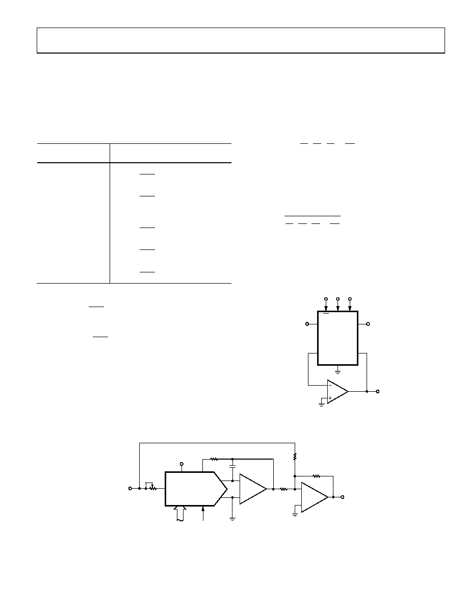
Bipolar Operation (4-Quadrant)
Figure 19 details a suggested circuit for bipolar, or offset binary,
operation. Table 7 shows the digital input to analog output
relationship. The circuit uses offset binary coding. Twos comple-
ment code can be converted to offset binary by software
inversion of the MSB or by the addition of an external inverter
to the MSB input.
Table 7. Bipolar (Offset Binary) Code Table1, 2
Digital Input
Nominal Analog Output
MSB
LSB
1111 1111 1111
2048
2047
REF
V
1000 0000 0001
2048
1
REF
V
1000 0000 0000
0
0111 1111 1111
2048
1
REF
V
0000 0000 0001
2048
2047
REF
V
0000 0000 0000
2048
REF
V
1 Nominal full scale for Figure 19 circuits is given by
2048
2047
REF
V
FS
2 Nominal LSB magnitude for Figure 19 circuits is given by
2048
1
REF
V
LSB
Resistors R3, R4, and R5 must be selected to match within 0.01%,
and they all must be of the same (preferably metal foil) type to
ensure temperature coefficient matching. Mismatching between
R3 and R4 causes offset and full-scale errors, while an R5 to R4
and R3 mismatch results in full-scale error.
Calibration is performed by loading the DAC register with 1000
0000 0000 and adjusting R1 until VOUT = 0 V. R1 and R2 may be
omitted, adjusting the ratio of R3 to R4 to yield VOUT = 0 V. Full
scale can be adjusted by loading the DAC register with 1111
1111 1111 and either adjusting the amplitude of VREF or the
value of R5 until the desired VOUT is achieved.
Analog/Digital Division
The transfer function for the DAC8043 connected in the
multiplying mode, as shown in Figure 16, Figure 17, and
Figure 19, is
12
3
2
1
2
...
2
12
3
2
1
IN
O
A
V
where AX assumes a value of 1 for an on bit and 0 for an off bit.
The transfer function is modified when the DAC is connected
in the feedback of an operational amplifier, as shown in Figure 18
and becomes
4
3
2
1
2
...
2
12
3
2
1
IN
O
A
V
The previous transfer function is the division of an analog
voltage (VREF) by a digital word. The amplifier goes to the rails
with all bits off because division by zero is infinity. With all bits
on the gain is 1 (±1 LSB). The gain becomes 4096 with the LSB,
Bit 12, on.
DAC8043
RFB
VDD
5V
LD SRI CLK
VREF
IOUT
GND
DIGITAL
INPUT
VIN
00
271
-01
9
OP42
2
3
6
VOUT
Figure 18. Analog/Digital Divider
00
27
1-
0
18
VOUT
CONTROL
INPUTS
SERIAL
DATA
INPUT
ANALOG
COMMON
VIN
R2
50
R3
10k
5V
R4
20k
R5
20k
R1
100
C1
10.33pF
1/2
OP200
A2
DAC8043
RFB
VDD
VREF
IOUT
GND
CONTROL
BITS
SRI
1/2
OP200
A1
Figure 19. Bipolar Operation (4-Quadrant, Offset Binary)
发布紧急采购,3分钟左右您将得到回复。
相关PDF资料
DAC8221GP
IC DAC 12BIT DUAL W/BUFF 24-DIP
DAC8222GPZ
IC DAC 12BIT DUAL W/BUFF 24DIP
DAC8229FSZ-REEL
IC DAC 8BIT DUAL V-OUT 20SOIC
DAC8248FS
IC DAC 12BIT DUAL W/BUFF 24-SOIC
DAC8408GP
IC DAC 8BIT QUAD W/MEMORY 28-DIP
DAC8413EP
IC DAC 12BIT QUAD V-OUT 28-DIP
DAC8420FQ
IC DAC 12BIT QUAD SRL LP 16-CDIP
DAC8426EPZ
IC DAC 8BIT QUAD 10VREF 20PDIP
相关代理商/技术参数
DAC8043GPZ
功能描述:IC DAC 12BIT MULTIPLY CMOS 8-DIP RoHS:是 类别:集成电路 (IC) >> 数据采集 - 数模转换器 系列:- 产品培训模块:Data Converter Fundamentals
DAC Architectures 标准包装:750 系列:- 设置时间:7µs 位数:16 数据接口:并联 转换器数目:1 电压电源:双 ± 功率耗散(最大):100mW 工作温度:0°C ~ 70°C 安装类型:表面贴装 封装/外壳:28-LCC(J 形引线) 供应商设备封装:28-PLCC(11.51x11.51) 包装:带卷 (TR) 输出数目和类型:1 电压,单极;1 电压,双极 采样率(每秒):143k
DAC8043HP
制造商:Analog Devices 功能描述: 制造商:PMI/AD 功能描述:
DAC8043U
功能描述:数模转换器- DAC 12bit Multiply D/A RoHS:否 制造商:Texas Instruments 转换器数量:1 DAC 输出端数量:1 转换速率:2 MSPs 分辨率:16 bit 接口类型:QSPI, SPI, Serial (3-Wire, Microwire) 稳定时间:1 us 最大工作温度:+ 85 C 安装风格:SMD/SMT 封装 / 箱体:SOIC-14 封装:Tube
DAC8043U
制造商:Texas Instruments 功能描述:D/A Converter (D-A) IC 制造商:Texas Instruments 功能描述:IC, DAC, 12BIT, 284KSPS, SOIC-8
DAC8043U/2K5
功能描述:数模转换器- DAC 12bit Multiply D/A RoHS:否 制造商:Texas Instruments 转换器数量:1 DAC 输出端数量:1 转换速率:2 MSPs 分辨率:16 bit 接口类型:QSPI, SPI, Serial (3-Wire, Microwire) 稳定时间:1 us 最大工作温度:+ 85 C 安装风格:SMD/SMT 封装 / 箱体:SOIC-14 封装:Tube
DAC8043U/2K5G4
功能描述:数模转换器- DAC 12bit Multiply D/A RoHS:否 制造商:Texas Instruments 转换器数量:1 DAC 输出端数量:1 转换速率:2 MSPs 分辨率:16 bit 接口类型:QSPI, SPI, Serial (3-Wire, Microwire) 稳定时间:1 us 最大工作温度:+ 85 C 安装风格:SMD/SMT 封装 / 箱体:SOIC-14 封装:Tube
DAC8043U2K5
制造商:TI 制造商全称:Texas Instruments 功能描述:CMOS 12-Bit Serial Input Multiplying DIGITAL-TO-ANALOG CONVERTER
DAC8043U2K5G4
制造商:TI 制造商全称:Texas Instruments 功能描述:CMOS 12-Bit Serial Input Multiplying DIGITAL-TO-ANALOG CONVERTER